| CPC G01R 15/148 (2013.01) [H10N 52/01 (2023.02); H10N 52/101 (2023.02); H10N 52/80 (2023.02)] | 9 Claims |

|
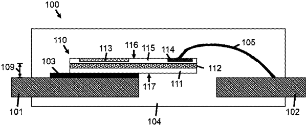
1. An integrated sensor die having a first and a second major surface, the second major surface being opposite to the first major surface;
the integrated sensor die comprising at least one magnetic field sensing element arranged on said first major surface of the integrated sensor die and suitable for sensing a magnetic field caused by a current flow;
wherein the integrated sensor die comprises a first insulation layer positioned between the first major surface and the second major surface such that it is substantially buried in the integrated sensor die;
wherein the integrated sensor die comprises a semiconductor-insulator-semiconductor substrate, wherein the insulator forms the first insulation layer and is bounded by a semiconductor material on both sides.
|