| CPC G01R 15/06 (2013.01) [G01R 19/0084 (2013.01); G01R 27/14 (2013.01)] | 20 Claims |
|
1. A voltage dividing device for dividing a voltage output from a voltage source, the voltage dividing device comprising:
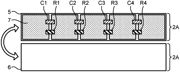
a plurality of resistive voltage dividing boards each being a plate-like board having a first face, the board having a plurality of conductor patterns arranged on the first face, the conductor patterns being connected in series with one another through capacitors and resistors connected in parallel on the first face, wherein
adjacent ones of the resistive voltage dividing boards are connected in series with each other through a conductive member, the adjacent resistive voltage dividing boards including one resistive voltage dividing board having a first face and a second face located rearwardly of the first face, and
the adjacent resistive voltage dividing boards are arranged such that the second face of the one resistive voltage dividing board and a first face of the other of the adjacent resistive voltage dividing boards face each other, and that the conductor patterns arranged on the first face of the one resistive voltage dividing board are disposed oppositely from the conductor patterns arranged on the first face of the other resistive voltage dividing board with the one resistive voltage dividing board disposed therebetween.
|