| CPC G01N 27/4145 (2013.01) [H01L 29/1606 (2013.01); H01L 29/66045 (2013.01)] | 22 Claims |
|
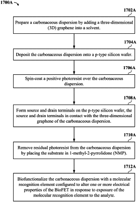
1. A method of fabricating a biological field-effect transistor (BioFET), the method comprising:
preparing a carbonaceous dispersion by adding a three-dimensional (3D) graphene into a solvent;
depositing the carbonaceous dispersion onto a p-type silicon wafer;
spin-coating a positive photoresist over the carbonaceous dispersion by placing a photomask with an image of an array of graphene field effect transistors (FETs) over the p-type wafer and exposing the p-type wafer to ultraviolet (UV) light;
forming source and drain terminals on the p-type silicon wafer, the source and drain terminals in contact with the 3D graphene of the carbonaceous dispersion;
removing residual photoresist from the carbonaceous dispersion by placing the p-type silicon wafer in 1-methyl-2-pyrrolidone (NMP); and
biofunctionalizing the carbonaceous dispersion with a molecular recognition element configured to alter one or more electrical properties of the Bio-FET in response to exposure of the molecular recognition element to the analyte.
|