| CPC G01N 21/9501 (2013.01) [G01N 21/8806 (2013.01); G03F 7/70608 (2013.01); H01L 22/12 (2013.01)] | 15 Claims |
|
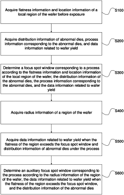
1. A method for determining a focus spot window of a wafer, comprising:
acquiring flatness information and location information of a local region of the wafer before exposure;
acquiring distribution information of abnormal dies, process information corresponding to the abnormal dies, and data information related to wafer yield; and
determining a focus spot window corresponding to a process according to the flatness information and the location information of the local region of the wafer, the distribution information of the abnormal dies, the process information corresponding to the abnormal dies, and the data information related to wafer yield;
wherein the data information related to wafer yield comprises a wafer yield test result map, wafer yield calculation methods, or wafer yield data values comprising a loss rate or a defect rate;
wherein the determining a focus spot window corresponding to a process according to the flatness information and the location information of the local region of the wafer, the distribution information of the abnormal dies, the process information corresponding to the abnormal dies, and the data information related to wafer yield comprises:
drawing a relation curve between the data information related to wafer yield and flatness of the local region of the wafer corresponding to the process according to the flatness information and the location information of the local region of the wafer, the distribution information of the abnormal dies, the process information corresponding to the abnormal dies, and the data information related to wafer yield; and
determining the focus spot window corresponding to the process according to the relation curve between the data information related to wafer yield and the flatness of the local region of the wafer corresponding to the process.
|