| CPC G01J 5/12 (2013.01) [G01J 5/045 (2013.01); G01J 5/0802 (2022.01); H01L 27/14618 (2013.01); H01L 27/14632 (2013.01); H01L 27/14649 (2013.01); H01L 27/14687 (2013.01); G01J 2005/106 (2013.01)] | 17 Claims |
|
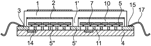
1. A method for producing a thermal infrared sensor array in a vacuum-filled wafer-level housing comprising at least two wafers,
a cover wafer (1) and
a central wafer (3) having a plurality of infrared-sensitive pixels (5) respectively on a slitted membrane (5″) over a thermally insulating cavity (11),
the method comprising:
initially providing the cover wafer (1) on an inner side with at least one cavity (10);
firmly mechanically connecting the cover wafer (1) to the central wafer (3) having the plurality of infrared-sensitive pixels (5) by wafer bonding;
subsequently thinning the central wafer (3) from a backside of the wafer to a predetermined thickness;
fastening a bottom wafer (4) on the backside of the central wafer (3) by wafer bonding; and
thinning the bottom wafer (4) after the wafer bonding.
|