| CPC G01J 1/4228 (2013.01) [G01J 1/46 (2013.01); G01J 3/2803 (2013.01); G01J 5/22 (2013.01); G01J 2001/4446 (2013.01)] | 13 Claims |
|
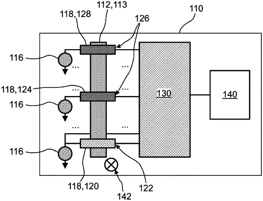
1. A device comprising:
at least one array of photoconductors, wherein each photoconductor is configured for exhibiting an electrical resistance dependent on an illumination of a light-sensitive region of each photoconductor, wherein at least one photoconductor of the at least one array of photoconductors is designed as a characterizing photoconductor;
at least one bias voltage source, wherein the bias voltage source is configured for applying at least one alternating bias voltage to the characterizing photoconductor or at least one direct current (DC) bias voltage to the characterizing photoconductor;
at least one photoconductor readout circuit, wherein the photoconductor readout circuit is configured for determining of a response voltage of the characterizing photoconductor generated in response to the bias voltage, wherein the response voltage is proportional to a variable characterizing the at least one array of photoconductors, wherein the variable characterizing the at least one array of photoconductors is at least one variable selected from a group consisting of dark resistance Rdark, signal noise, and signal response to a known intensity, wherein the photoconductor readout circuit is configured for determining of the response voltage of the characterizing photoconductor during operation of the at least one array of photoconductors; and
at least one evaluation device, wherein the evaluation device is configured for determining responsivity R from the signal response to the known intensity and detectivity D* from the signal response to the known intensity and from signal noise.
|