| CPC G01B 11/0625 (2013.01) [G01B 5/06 (2013.01); G01B 11/02 (2013.01); G01B 11/06 (2013.01); G02B 17/0816 (2013.01); G02B 17/0868 (2013.01)] | 11 Claims |
|
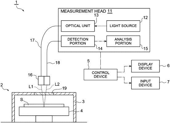
1. An optical unit comprising:
an input portion comprising an aperture configured to have light having a wavelength extending from an ultraviolet region to a visible region input thereto;
an optical system comprising one or more optical elements configured to condense the light in a state where a chromatic aberration is caused to occur; and
an opening portion comprising an input end toward an optical fiber configured not to image light having a wavelength in the visible region and to image light having a wavelength in the ultraviolet region of the light having the chromatic aberration having occurred therein.
|