| CPC C30B 29/36 (2013.01) [C30B 23/002 (2013.01); C30B 23/066 (2013.01); H01L 29/1608 (2013.01)] | 5 Claims |
|
1. A manufacturing method of a silicon carbide wafer, comprising:
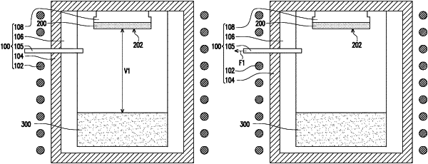
providing a raw material containing carbon and silicon and a seed located above the raw material in a reactor;
reducing a nitrogen content in the reactor, comprising:
performing a first vacuum process on the reactor, such that an air pressure in the reactor is 0.1 torr to 100 torr;
after the first vacuum process, passing an argon gas into the reactor, wherein a flow rate of passing the argon gas into the reactor is 1,000 sccm to 5,000 sccm, and a time of passing the argon gas into the reactor is 2 hours to 48 hours; and
after passing the argon gas into the reactor, performing a second vacuum process on the reactor, such that an air pressure in the reactor is less than 5×10⁻⁵ torr;
heating the reactor and the raw material to form a silicon carbide material on the seed;
cooling the reactor and the raw material to obtain a silicon carbide ingot; and
cutting the silicon carbide ingot to obtain a plurality of silicon carbide wafers, wherein a resistivity of each of the silicon carbide wafers is 0.1 ohm/cm to 10 ohms/cm, wherein a visible light transmittance of each of the silicon carbide wafers is greater than 50%.
|