| CPC C30B 29/06 (2013.01) [C30B 15/007 (2013.01); C30B 15/04 (2013.01); C30B 15/14 (2013.01); C30B 15/203 (2013.01); C30B 29/66 (2013.01); C30B 25/10 (2013.01); C30B 25/20 (2013.01)] | 7 Claims |
|
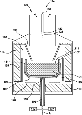
1. A method for forming a silicon substrate with reduced grown-in nuclei for epitaxial defects, the method comprising:
adding an initial charge of polycrystalline silicon to a crucible disposed in an ingot puller apparatus;
heating the crucible comprising the initial charge of polycrystalline silicon to cause a silicon melt to form in the crucible;
adding a single dopant to the crucible, the single dopant being boron, boron being added to the crucible to prepare a doped silicon melt having a boron concentration of at least 3.8×10¹⁸ atoms/cm3;
contacting a silicon seed crystal with the doped silicon melt;
withdrawing the silicon seed crystal to grow a single crystal silicon ingot, the ingot having a constant diameter portion;
controlling (i) a growth velocity, v, and/or (ii) an axial temperature gradient, G, during the growth of a segment of the constant diameter portion of the ingot having a boron concentration of less than 8.0×10¹⁸ atoms/cm3, the ratio of v/G being controlled such that the ratio v/G is less than a critical v/G and interstitials are the dominant intrinsic point defect in the segment;
pulling the segment through a hotzone of the ingot puller apparatus, the segment of the constant diameter portion of the ingot being cooled from its solidification temperature to 950° C. or less as the segment is pulled through the hotzone, wherein the dwell time the segment of the constant diameter portion of the ingot is in the temperature range from 1150° C. to 950° C. is less than 160 minutes; and
slicing the substrate from the single crystal silicon ingot.
|