| CPC C23C 16/4404 (2013.01) [C23C 4/134 (2016.01); G01N 23/20 (2013.01); H01J 37/32495 (2013.01); H01L 21/3065 (2013.01); H01J 2237/332 (2013.01); H01J 2237/334 (2013.01)] | 16 Claims |
|
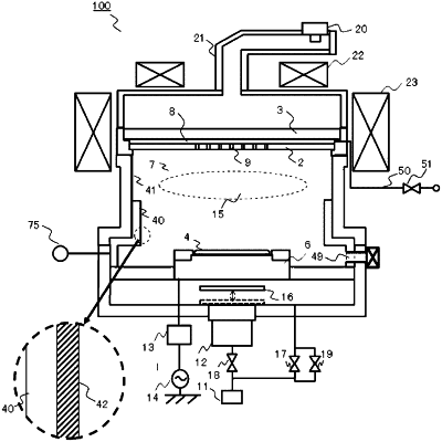
1. A manufacturing method of an interior member which is arranged inside a processing chamber disposed inside a vacuum container of a plasma processing apparatus configured to process a wafer by using plasma formed in the processing chamber, and which includes, on a surface of said interior member, a first film of a material having resistance to the plasma, the manufacturing method of the interior member comprising:
a step of forming the first film by spraying the material onto the surface of the interior member by moving a gun by a predetermined distance along the surface of the interior member, and forming a second film by spraying the material on a surface of a test piece which has a shape simulating a surface shape of the interior member and which is disposed within a range of the predetermined distance, by moving the gun within the predetermined distance; and
a step of adjusting a condition of forming the first film on the surface of the interior member by the gun, based on a result of detecting at least one of a crystal size of the second film on the surface of the test piece, a residual stress, and a contaminant element.
|