| CPC C23C 16/303 (2013.01) [C23C 14/48 (2013.01); C23C 16/40 (2013.01); C23C 16/513 (2013.01); C23C 28/04 (2013.01); H01L 21/30604 (2013.01); H01L 21/30621 (2013.01); H01L 21/3065 (2013.01)] | 20 Claims |
|
1. A method, comprising:
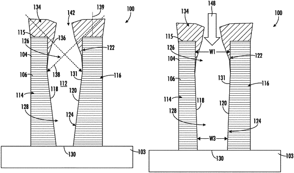
providing a set of semiconductor structures defining an opening, wherein the opening has a first opening width along an upper portion of the opening and a second opening width along a lower portion of the opening, and wherein the first opening width is greater than the second opening width; and
forming a blocking layer along the set of semiconductor structures by delivering a material at a non-zero angle of inclination relative to a normal extending perpendicular from a top surface of the set of semiconductor structures, wherein the blocking layer is formed along the upper portion of the opening without being formed along the lower portion of the opening, and wherein an opening through the blocking layer is present above the opening.
|
|
9. A method of forming a memory hole in a semiconductor device, the method comprising:
providing a set of semiconductor structures defining the memory hole, wherein the memory hole has a first opening width along an upper portion of the opening and a second opening width along a lower portion of the opening, and wherein the first opening width is greater than the second opening width;
forming a blocking layer along the set of semiconductor structures by:
delivering a material at a first non-zero angle of inclination relative to a normal extending perpendicular from a top surface of the set of semiconductor structures; and
delivering the material at a second non-zero angle of inclination relative to the normal extending perpendicular from the top surface of the set of semiconductor structures, wherein the blocking layer is formed along the upper portion of the memory hole without being formed along the lower portion of the memory hole, and wherein an opening through the blocking layer is present above the memory hole; and
etching the lower portion of the memory hole following formation of the blocking layer, wherein etching the lower portion of the opening increase the second opening width.
|
|
15. A method of forming a memory device, comprising:
providing a pair of semiconductor structures each having a sidewall defining a via, wherein the via has a first opening width along an upper portion of the sidewalls and a second opening width along a lower portion of the sidewalls, and wherein the first opening width is greater than the second opening width;
forming a blocking layer along the upper portion of the sidewalls of the pair of semiconductor structures by:
delivering a material at a first non-zero angle of inclination relative to a normal extending perpendicular from a top surface of the pair of semiconductor structures; and
delivering the material at a second non-zero angle of inclination relative to the normal extending perpendicular from the top surface of the pair of semiconductor structures, wherein the blocking layer is prevented from being formed along the lower portion of the sidewalls of the pair of semiconductor structures, and wherein an opening through the blocking layer is present above the via; and
etching, following formation of the blocking layer, the lower portion of the sidewalls of the pair of semiconductor structures to increase the second opening width.
|