US 11,987,876 B2
Chamfer-less via integration scheme
Sivananda Krishnan Kanakasabapathy, Pleasanton, CA (US); Hui-Jung Wu, Pleasanton, CA (US); Richard Wise, Los Gatos, CA (US); and Arpan Mahorowala, West Linn, OR (US)
Assigned to Lam Research Corporation, Fremont, CA (US)
Appl. No. 16/982,489
Filed by Lam Research Corporation, Fremont, CA (US)
PCT Filed Mar. 14, 2019, PCT No. PCT/US2019/022319
§ 371(c)(1), (2) Date Sep. 18, 2020,
PCT Pub. No. WO2019/182872, PCT Pub. Date Sep. 26, 2019.
Claims priority of provisional application 62/644,783, filed on Mar. 19, 2018.
Prior Publication US 2021/0017643 A1, Jan. 21, 2021
Int. Cl. C23C 16/04 (2006.01); C23C 16/40 (2006.01); C23C 16/455 (2006.01); H01L 21/311 (2006.01); H01L 21/67 (2006.01); H01L 21/768 (2006.01)
CPC C23C 16/045 (2013.01) [C23C 16/407 (2013.01); C23C 16/45553 (2013.01); H01L 21/31122 (2013.01); H01L 21/31144 (2013.01); H01L 21/67023 (2013.01); H01L 21/67069 (2013.01); H01L 21/76808 (2013.01)] 27 Claims
OG exemplary drawing
 
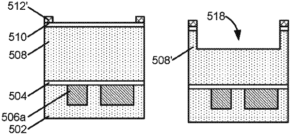
1. A method comprising:
providing a substrate having a trench formed in a dielectric material;
depositing a selectively removable sealant layer conformally in the trench,
wherein the selectively removable sealant layer comprises a Group IV metal;
forming a patterned hard mask on the selectively removable sealant layer;
etching the dielectric material using the patterned hard mask; and
removing the patterned hard mask and the selectively removable sealant layer to produce a chamferless via.