| CPC C23C 16/0227 (2013.01) [C23C 16/04 (2013.01); C23C 16/56 (2013.01); C23C 22/77 (2013.01); C23C 22/82 (2013.01)] | 12 Claims |
|
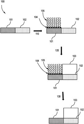
1. A semiconductor device patterning method comprising:
in a substrate processing chamber, exposing a semiconductor device substrate surface including a metal surface and a dielectric surface to a vapor phase heterocyclic reactant comprising a heterocyclic headgroup selected from the group consisting of a phosphinine group, a phosphinoline group, and a phosphole group, and a tailgroup comprising a carbon chain having a length in the range of from 1 to 50 carbon atoms;
in the substrate processing chamber, selectively depositing the vapor phase heterocyclic reactant on the metal surface to cover the metal surface with a blocking layer, wherein the heterocyclic headgroup selectively binds to the metal surface;
in the substrate processing chamber, depositing a dielectric material on the dielectric surface not covered by the blocking layer at a dielectric deposition temperature up to 350° C. at which the heterocyclic reactant remains bound to the metal surface and maintains stability; and
decomposing the blocking layer covering the metal surface in the substrate processing chamber at temperature higher than the dielectric deposition temperature to form a pattern on the semiconductor device substrate surface.
|