| CPC C23C 14/18 (2013.01) [C23C 14/243 (2013.01); C23C 14/5873 (2013.01)] | 19 Claims |
|
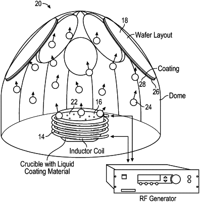
1. A method of forming a metal layer on a semiconductor wafer, the method comprising:
placing a semiconductor wafer into an evaporator dome, the semiconductor wafer comprising an average thickness of less than 39 microns;
adding a material to a crucible located a predetermined distance from the semiconductor wafer;
heating the material in the crucible to a vapor; and
depositing the material on a second side of the semiconductor wafer.
|