| CPC B81B 7/0058 (2013.01) [B81C 1/00333 (2013.01); B81B 2203/0307 (2013.01)] | 20 Claims |
|
1. A method for forming a microelectromechanical systems (MEMS) package, wherein the method comprises:
mounting a support substrate on a package substrate;
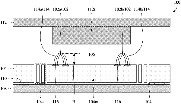
mounting a MEMS structure on the support substrate, wherein the MEMS structure comprises a movable mass configured to move over the support substrate, and further comprises a first conductive pad and a second conductive pad that are on a top of the movable mass and that are laterally spaced from each other;
performing one or more wire-bonding processes to form an out-of-plane (OoP) wire-bond damper on a top surface of the movable mass; and
mounting a housing structure to the package substrate, wherein the housing structure covers and surrounds the MEMS structure;
wherein the OoP wire-bond damper is formed comprising a first arch-shaped wire, and wherein a first wire-bonding process of the one or more wire-bonding processes forms the first arch-shaped wire arching continuously from direct contact with the first conductive pad to direct contact with the second conductive pad.
|