| CPC B32B 3/30 (2013.01) [B32B 3/263 (2013.01); B32B 7/12 (2013.01); B32B 15/08 (2013.01); B32B 15/09 (2013.01); B32B 15/20 (2013.01); B32B 27/06 (2013.01); B32B 27/281 (2013.01); B32B 27/36 (2013.01); H05K 3/281 (2013.01); B32B 2250/03 (2013.01); B32B 2307/202 (2013.01); B32B 2307/206 (2013.01); B32B 2307/51 (2013.01); B32B 2405/00 (2013.01); B32B 2457/08 (2013.01); B32B 2457/10 (2013.01); B32B 2457/20 (2013.01); B32B 2571/00 (2013.01); H05K 3/285 (2013.01); H05K 3/387 (2013.01); H05K 2201/0129 (2013.01); H05K 2201/0145 (2013.01); H05K 2201/0154 (2013.01); H05K 2201/0191 (2013.01); H05K 2201/0195 (2013.01); H05K 2203/0557 (2013.01)] | 22 Claims |
|
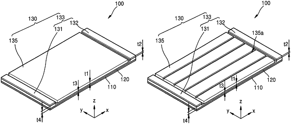
1. A protection tape for a printed circuit board (PCB), the protection tape comprising:
an insulating base plate;
a conductive layer over the insulating base plate; and
an adhesive layer over the conductive layer, the adhesive layer being a pressure sensitive adhesive (PSA) and including a main part having a first thickness and a subsidiary part having a second thickness less than the first thickness, the main part corresponding to at least a center portion of the insulating base plate and the subsidiary part being arranged at an outside of the main part, wherein
the conductive layer has an integral one-piece form consisting of a common material and includes a center part having a third thickness, and an edge part having a fourth thickness greater than the third thickness, the center part of the conductive layer corresponding to the main part of the adhesive layer and the edge part corresponding to the subsidiary part of the adhesive layer.
|