US 11,986,267 B2
Microscopy imaging device with advanced imaging properties
Kunal Ghosh, San Francisco, CA (US); Laurie D. Burns, Menlo Park, CA (US); Abbas El Gamal, Palo Alto, CA (US); Mark J. Schnitzer, Palo Alto, CA (US); Eric Cocker, Palo Alto, CA (US); and Tatt Wei Ho, Stanford, CA (US)
Assigned to The Board of Trustees of the Leland Stanford Junior University, Stanford, CA (US)
Filed by The Board of Trustees of the Leland Stanford Junior University, Stanford, CA (US)
Filed on Aug. 26, 2022, as Appl. No. 17/896,461.
Application 17/896,461 is a continuation of application No. 17/581,019, filed on Jan. 21, 2022, abandoned.
Application 17/581,019 is a continuation of application No. 17/080,295, filed on Oct. 26, 2020, granted, now 11,259,703, issued on Mar. 1, 2022.
Application 17/080,295 is a continuation of application No. 15/444,049, filed on Feb. 27, 2017, granted, now 10,813,552, issued on Oct. 27, 2020.
Application 15/444,049 is a continuation of application No. 14/857,156, filed on Sep. 17, 2015, granted, now 9,629,554, issued on Apr. 25, 2017.
Application 14/857,156 is a continuation of application No. 13/218,181, filed on Aug. 25, 2011, granted, now 9,195,043, issued on Nov. 24, 2015.
Claims priority of provisional application 61/377,591, filed on Aug. 27, 2010.
Prior Publication US 2023/0200656 A1, Jun. 29, 2023
Int. Cl. A61B 5/00 (2006.01); A61B 90/20 (2016.01); G01N 21/64 (2006.01); G02B 3/00 (2006.01); G02B 21/00 (2006.01); G02B 21/16 (2006.01); G02B 21/36 (2006.01); G02B 27/14 (2006.01); G06T 7/00 (2017.01); H04N 23/55 (2023.01); H04N 23/56 (2023.01); H04N 23/69 (2023.01); A61B 90/30 (2016.01)
CPC A61B 5/0071 (2013.01) [A61B 90/20 (2016.02); G01N 21/6458 (2013.01); G02B 3/0087 (2013.01); G02B 21/0008 (2013.01); G02B 21/008 (2013.01); G02B 21/16 (2013.01); G02B 21/36 (2013.01); G02B 21/361 (2013.01); G02B 21/362 (2013.01); G02B 21/365 (2013.01); G02B 27/141 (2013.01); G06T 7/0012 (2013.01); H04N 23/55 (2023.01); H04N 23/56 (2023.01); H04N 23/69 (2023.01); A61B 5/0042 (2013.01); A61B 5/0082 (2013.01); A61B 5/489 (2013.01); A61B 2090/306 (2016.02); A61B 2503/40 (2013.01); A61B 2503/42 (2013.01); A61B 2562/0233 (2013.01); A61B 2562/04 (2013.01); A61B 2576/026 (2013.01); G06T 2207/30016 (2013.01); G06T 2207/30101 (2013.01)] 10 Claims
OG exemplary drawing
 
1. A method comprising:
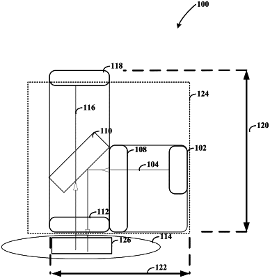
upon removably connecting an epifluorescence microscopy system, which has a dimension not exceeding 1 inch along an axis parallel to a specimen plane, to a support structure that has been affixed to a target object, directing first light from a light source through an optical excitation arrangement of the epifluorescence microscopy system towards a pre-defined area at the specimen plane in the target object;
with an imaging circuit of the microscopy system that includes an optical sensor array, receiving fluorescence generated at the pre-defined area as a result of said directing to generate image data; and
with a synchronization circuit of the microscopy system, comparing said image data with information representing visual feedback generated outside the epifluorescence microscopy system to transform parameters of said directing first light, wherein the synchronization circuit is in operable communication with the imaging circuit.