| CPC H01L 21/76897 (2013.01) [H01L 29/42372 (2013.01)] |
| AS A RESULT OF REEXAMINATION, IT HAS BEEN DETERMINED THAT: |
| The patentability of claims 5-8 and 10-11 is confirmed. |
| Claims 1-4, 9, and 12-20 were not reexamined. |
|
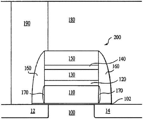
5. A semiconductor structure, comprising;
a semiconductor substrate,
a gate layer, on the semiconductor substrate,
a metallic layer, on the gate layer,
an etch-stop layer, on the metallic layer,
an insulating layer, on the etch-stop layer, and on the substrate, and
a via, through the insulating layer, on the substrate,
wherein an area of contact between the via and the substrate has a via width,
the via width is at most 0.12 micron,
a distance between the substrate and a top of the etch-stop layer has a gate stack height, and
the gate stack height is at most 2700 angstroms.
|