US 11,985,905 B2
Highly physical ion resistive spacer to define chemical damage free sub 60nm MRAM devices
Yi Yang, Fremont, CA (US); Dongna Shen, San Jose, CA (US); and Yu-Jen Wang, San Jose, CA (US)
Assigned to TAIWAN SEMICONDUCTOR MANUFACTURING COMPANY, LTD., Hsinchu (TW)
Filed by Taiwan Semiconductor Manufacturing Company, Ltd., Hsin-Chu (TW)
Filed on Jan. 23, 2023, as Appl. No. 18/158,086.
Application 17/216,016 is a division of application No. 15/986,244, filed on May 22, 2018, granted, now 10,964,887, issued on Mar. 30, 2021.
Application 18/158,086 is a continuation of application No. 17/216,016, filed on Mar. 29, 2021, granted, now 11,563,171.
Prior Publication US 2023/0165157 A1, May 25, 2023
Int. Cl. H10N 50/10 (2023.01); G11C 11/16 (2006.01); H01F 10/32 (2006.01); H01F 41/34 (2006.01); H10N 50/01 (2023.01); H10N 50/80 (2023.01); H01F 41/30 (2006.01)
CPC H10N 50/01 (2023.02) [G11C 11/161 (2013.01); H01F 10/3254 (2013.01); H01F 41/34 (2013.01); H10N 50/10 (2023.02); H10N 50/80 (2023.02)] 20 Claims
OG exemplary drawing
 
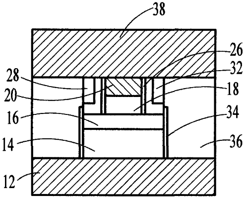
1. A device comprising:
a stack of magnetic tunneling junction (MTJ) layers, the stack of MTJ layers including a first portion having a first width and a second portion having a second width that is different than the first width, the second portion disposed over the first portion of the stack of MTJ layers;
a first metal re-deposition layer disposed directly on a surface of the first portion of the stack of MTJ layers;
a second metal re-deposition layer disposed directly on a surface of the second portion of the stack of MTJ layers;
a dielectric layer extending from the second metal re-deposition layer to the first metal re-deposition layer; and
a spacer disposed directly on the dielectric layer.