| CPC H10K 59/60 (2023.02) [G02F 1/136209 (2013.01); H10K 59/879 (2023.02); H10K 59/8792 (2023.02)] | 20 Claims |
|
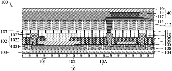
1. An array substrate, comprising:
a substrate;
a photosensitive element, disposed on the substrate and comprising a doped semiconductor layer made of polysilicon, an intrinsic semiconductor layer made of amorphous silicon, and a transparent electrode layer sequentially stacked;
a first insulating layer, disposed on a side of the doped semiconductor layer facing away from the substrate, extending to the substrate, and provided with a first via hole; and
a second insulating layer, disposed on a side of the intrinsic semiconductor layer facing away from the substrate, extending to the first insulating layer, and provided with a second via hole,
wherein the intrinsic semiconductor layer is disposed on a side of the first insulating layer away from the substrate and is connected to the doped semiconductor through the first via hole, and the transparent electrode layer is disposed on a side of the second insulating layer away from the doped semiconductor layer and is connected to the intrinsic semiconductor layer through the second via hole; and
wherein the doped semiconductor layer is an N-type doped semiconductor, and the transparent electrode layer is a P-type transparent electrode, or the doped semiconductor layer is a P-type doped semiconductor, and the transparent electrode layer is an N-type transparent electrode.
|