| CPC H10K 59/1315 (2023.02) [H10K 77/111 (2023.02); H01L 29/78603 (2013.01); H01L 29/78633 (2013.01); H10K 2102/311 (2023.02)] | 15 Claims |

|
1. A display device comprising:
a resin substrate on which a display area where an image is displayed and a frame area surrounding the display area are specified;
a thin film transistor (TFT) layer on the resin substrate;
a terminal section along a side of the frame area;
a bending portion extending in a first direction between the display area and the terminal section;
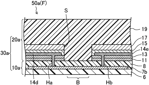
a stack of inorganic insulation films on the resin substrate, the inorganic insulation films partially forming the TFT layer and having a slit formed therethrough in the bending portion to expose a top face of the resin substrate; and
a plurality of first overlying wires on any one of the inorganic insulation films, the plurality of first overlying wires, partially forming the TFT layer and between the display area and the bending portion, extending parallel to each other in a second direction crossing the first direction, wherein
the resin substrate includes:
a first resin layer in the display area and the frame area opposite the TFT layer;
a plurality of underlying wires on a TFT layer side of the first resin layer in the frame area, the plurality of underlying wires extending across the slit and parallel to each other in the second direction; and
a second resin layer on the TFT layer side of the first resin layer in the display area and the frame area, the second resin layer covering the plurality of underlying wires, and
the plurality of first overlying wires is electrically connected, respectively, to the plurality of underlying wires via a plurality of first contact holes, formed through the second resin layer and the inorganic insulation films, residing between the plurality of first overlying wires and the plurality of underlying wires.
|