| CPC H10K 59/131 (2023.02) [H10K 59/1213 (2023.02); H10K 59/1216 (2023.02); H10K 59/353 (2023.02)] | 23 Claims |
|
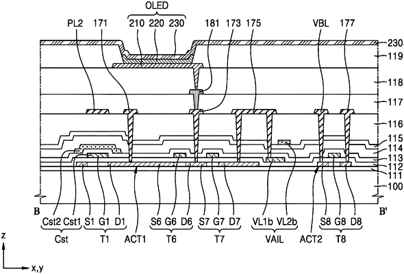
1. A display panel comprising:
a substrate comprising a display area in which a plurality of pixels are arranged, and a peripheral area surrounding at least a portion of the display area;
a first semiconductor layer in the display area and comprising a first channel area;
a first conductive layer on the first semiconductor layer, the first conductive layer comprises a first electrode overlapping the first channel area;
a second conductive layer on the first conductive layer, the second conductive layer comprises a second electrode overlapping the first electrode and a first voltage line extending in a first direction;
a second semiconductor layer on the second conductive layer, the second semiconductor layer comprises a second channel area;
a third conductive layer on the second semiconductor layer, the third conductive layer comprises a third electrode overlapping the second channel area and a second voltage line overlapping the first voltage line; and
a fourth conductive layer on the third conductive layer, the fourth conductive layer comprises a third voltage line and a fourth voltage line extending in a second direction intersecting the first direction;
wherein each of the plurality of pixels comprises a first sub-pixel configured to emit light of a first color and a second sub-pixel configured to emit light of a second color,
the first voltage line and the third voltage line are each configured to transmit a first initialization voltage to the first sub-pixel, and
the second voltage line and the fourth voltage line are each configured to transmit a second initialization voltage to the second sub-pixel.
|