| CPC H10K 59/126 (2023.02) [G06F 3/0446 (2019.05); H10K 50/844 (2023.02); H10K 59/40 (2023.02); H10K 59/65 (2023.02)] | 18 Claims |
|
1. A display apparatus comprising:
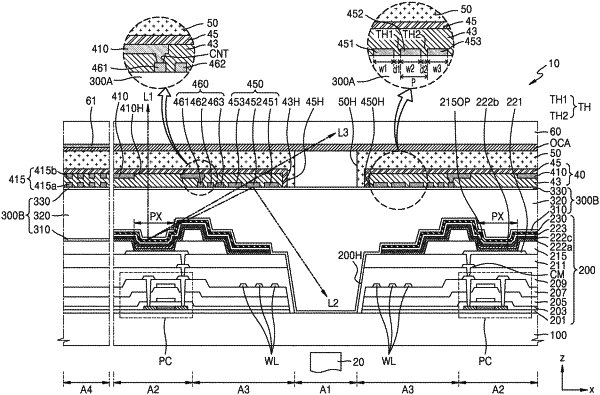
a substrate comprising a first area, a second area surrounding the first area and spaced apart from the first area, and a third area between the first area and the second area;
a plurality of pixel circuits on the substrate at the second area, each of the plurality of pixel circuits comprising one or more thin-film transistors, and a storage capacitor;
a plurality of lines on the substrate at the third area, and electrically connected to the pixel circuits, respectively;
an encapsulation member covering the pixel circuits;
an input sensing section on the encapsulation member to overlap with the second area, and comprising sensing electrodes, and trace lines electrically connected to the sensing electrodes;
a plurality of shielding portions on the encapsulation member to overlap with at least one of the plurality of lines, the plurality of shielding portions being spaced apart from each other; and
a plurality of metal wires on the encapsulation member to surround the plurality of shielding portions.
|