| CPC H10K 59/123 (2023.02) [H10K 50/84 (2023.02); H10K 50/865 (2023.02); H10K 59/38 (2023.02); H10K 59/40 (2023.02); H10K 71/00 (2023.02); H10K 59/1201 (2023.02)] | 6 Claims |
|
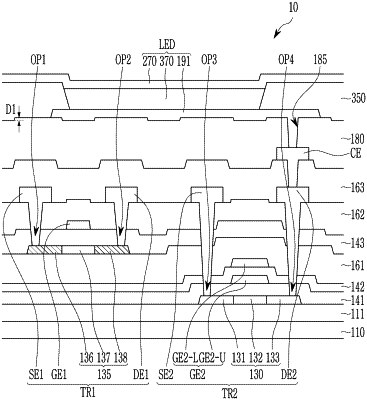
1. A display device comprising:
a substrate;
a polycrystalline semiconductor that is disposed on the substrate;
a first gate insulation layer that is disposed on the polycrystalline semiconductor;
a driving gate electrode that is disposed on the first gate insulating layer;
a second gate insulating layer that is disposed on the driving gate electrode;
a first interlayer insulation layer that is disposed on the second gate insulating layer;
an oxide semiconductor that is disposed on the first interlayer insulating layer;
a third gate insulating layer that is disposed on the oxide semiconductor;
a switching gate electrode that is disposed on the third gate insulating layer;
a second interlayer insulating layer that is disposed on the switching gate electrode;
a first source electrode and a first drain electrode that are disposed on the second interlayer insulating layer, and connected with the oxide semiconductor;
a second source electrode and a second drain electrode that are disposed on the second interlayer insulating layer, and connected to the polycrystalline semiconductor;
a light emitting diode that is disposed on the substrate, and connected to the second source electrode or the second drain electrode; and
a passivation layer that is disposed between the second interlayer insulating layer and the light emitting diode,
wherein a surface step of the passivation layer is within a range of and including 1 nm to 30 nm,
wherein the passivation layer comprises a first portion that overlaps the first source electrode, the first drain electrode, the second source electrode, and the second drain electrode, and a second portion that does not overlap the first source electrode, the first drain electrode, the second source electrode, and the second drain electrode, and
wherein a surface height of the first portion is higher than a surface height of the second portion.
|