| CPC H10K 59/122 (2023.02) [H10K 59/131 (2023.02)] | 18 Claims |
|
1. An array substrate, comprising:
a base substrate;
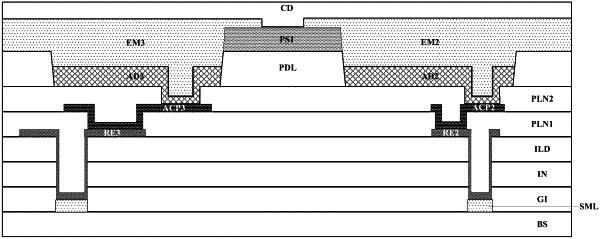
a pixel definition layer on the base substrate, the pixel definition layer defining subpixel apertures;
a spacer layer on a side of the pixel definition layer away from the base substrate, wherein the spacer layer comprises first spacers arranged in a first array and second spacers arranged in a second array;
adjacent spacers along a column direction are spaced apart from each other by a column distance;
adjacent spacer along a row direction are spaced apart from each other by a row distance;
the column distance is greater than the row distance;
wherein a second subpixel aperture, a third subpixel aperture, a fourth subpixel aperture respectively extending through the pixel definition layer, wherein a second light emitting layer, a third light emitting layer, and a fourth light emitting layer respectively connected to a second anode, a third anode, and a fourth anode, respectively through the second subpixel aperture, the third subpixel aperture, the fourth subpixel aperture;
a respective one of the first spacers is between the second subpixel aperture and the third subpixel aperture; and
a respective one of the second spacers is between the third subpixel aperture and the fourth subpixel aperture;
wherein the array substrate further comprises a plurality of pixel driving circuits respectively in a plurality of subpixels configured to respectively drive a plurality of light emitting elements;
wherein a respective one of the plurality of pixel driving circuits comprises a plurality of transistors, and a storage capacitor comprising a first capacitor electrode, a second capacitor electrode electrically connected to a respective voltage supply line, and an insulating layer between the first capacitor electrode and the second capacitor electrode;
wherein the array substrate comprises:
a semiconductor material layer on the base substrate; and
a node connecting line in a same layer as the respective voltage supply line, connected to the first capacitor electrode through a first via, and connected to the semiconductor material layer through a second via;
wherein an orthographic projection of a first anode of a first light emitting element in a respective first subpixel on the base substrate at least partially overlaps with an orthographic projection of a node connecting line in the respective first subpixel on the base substrate;
an orthographic projection of a second anode of a second light emitting element in a respective second subpixel on the base substrate at least partially overlaps with an orthographic projection of the node connecting line in the respective second subpixel on the base substrate;
an orthographic projection of a third anode of a third light emitting element in a respective third subpixel on the base substrate at least partially overlaps with an orthographic projection of the node connecting line in the respective third subpixel on the base substrate; and
an orthographic projection of a fourth anode of a fourth light emitting element in a respective fourth subpixel on the base substrate at least partially overlaps with an orthographic projection of the node connecting line in the respective fourth subpixel on the base substrate.
|