US 11,985,857 B2
Display device, method of manufacturing display device, and electronic apparatus
Hitoshi Tsuno, Kanagawa (JP)
Assigned to Sony Group Corporation, Tokyo (JP)
Filed by Sony Group Corporation, Tokyo (JP)
Filed on May 12, 2023, as Appl. No. 18/196,744.
Application 18/196,744 is a continuation of application No. 17/669,060, filed on Feb. 10, 2022, granted, now 11,678,519.
Application 17/669,060 is a continuation of application No. 17/079,939, filed on Oct. 26, 2020, granted, now 11,271,060, issued on Mar. 8, 2022.
Application 17/079,939 is a continuation of application No. 16/714,254, filed on Dec. 13, 2019, granted, now 10,840,319, issued on Nov. 17, 2020.
Application 16/714,254 is a continuation of application No. 16/380,522, filed on Apr. 10, 2019, granted, now 10,535,723, issued on Jan. 14, 2020.
Application 16/380,522 is a continuation of application No. 16/226,130, filed on Dec. 19, 2018, granted, now 10,573,700, issued on Feb. 25, 2020.
Application 16/226,130 is a continuation of application No. 15/323,651, granted, now 10,297,653, issued on May 21, 2019, previously published as PCT/JP2015/061962, filed on Apr. 20, 2015.
Claims priority of application No. 2014-149433 (JP), filed on Jul. 23, 2014.
Prior Publication US 2023/0354644 A1, Nov. 2, 2023
Int. Cl. H01L 21/00 (2006.01); H01L 21/28 (2006.01); H01L 21/66 (2006.01); H01L 27/12 (2006.01); H01L 29/41 (2006.01); H01L 29/786 (2006.01); H01L 29/788 (2006.01); H10K 59/121 (2023.01); H10K 59/131 (2023.01); H01L 21/265 (2006.01); H01L 21/285 (2006.01); H10K 59/12 (2023.01)
CPC H10K 59/1213 (2023.02) [H01L 21/28 (2013.01); H01L 22/20 (2013.01); H01L 27/1251 (2013.01); H01L 29/41 (2013.01); H01L 29/786 (2013.01); H01L 29/78645 (2013.01); H01L 29/78648 (2013.01); H01L 29/788 (2013.01); H10K 59/131 (2023.02); H01L 21/26513 (2013.01); H01L 21/28556 (2013.01); H01L 27/124 (2013.01); H01L 27/1274 (2013.01); H10K 59/1201 (2023.02)] 12 Claims
OG exemplary drawing
 
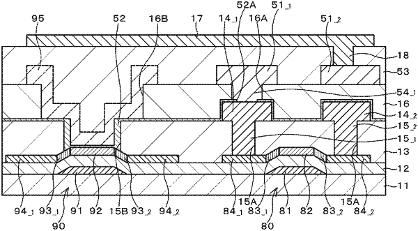
1. A display device comprising:
a substrate; and
a plurality of pixels arranged on the substrate, respective ones of the plurality of pixels including a light emitting element, a driving transistor, a sampling transistor, and a capacitor, wherein
the light emitting element includes a first electrode, an organic layer disposed on the first electrode, and a second electrode disposed on the organic layer,
the driving transistor includes a first gate electrode disposed over a channel region, a first source or drain region, a second source or drain region, and a metal layer being disposed under the channel region,
the sampling transistor includes a second gate electrode, a third source or drain region, and a fourth source or drain region, and
the third source or drain region of the sampling transistor is electrically connected to the gate electrode of the driving transistor.