| CPC H10K 59/1213 (2023.02) [H01L 25/167 (2013.01); H10K 50/805 (2023.02); H10K 50/84 (2023.02); H10K 2102/311 (2023.02)] | 20 Claims |
|
1. A light emitting device of a display apparatus, comprising:
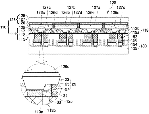
a light emitting region comprising a plurality of light emitters, each light emitter comprising:
a light emitting layer comprising a first conductivity type semiconductor layer, a second conductivity type semiconductor layer, and an active layer interposed between the first and second conductivity semiconductor layers;
a first electrode disposed on the first conductivity type semiconductor layer and electrically connected to the first conductivity type semiconductor layer; and
a second electrode disposed on the second conductivity type semiconductor layer and electrically connected to the second conductivity type semiconductor layer;
a divider disposed between at least two light emitters and configure to divide the light emitting region into a plurality of sub light emitting regions;
a connection substrate configured to support the plurality of light emitters and having an insulated region and a conductive region;
an encapsulation material filling the plurality of sub light emitting regions and disposed to cover a top surface of the connection substrate and surround side surfaces of the plurality of light emitters;
a protective layer disposed on the light emitting region and comprising a transparent material through which a light emitted from the plurality of light emitters passes,
wherein:
the connection substrate comprises a first conductive region electrically connected to the first electrode and a second conductive region electrically connected to the second electrode;
the first and second conductive regions include a material configured to reflect the light emitted from the plurality of light emitters;
the plurality of sub light emitting regions comprises a first light emitting region having a first peak wavelength, a second light emitting region having a second peak wavelength range which is longer than the first peak wavelength, and a third light emitting region having a third peak wavelength range which is longer than the first peak wavelength;
the divider is disposed between the first light emitting region and the third light emitting region; and
the encapsulation material is disposed between the connection substrate and the protective layer.
|