| CPC H10K 59/1213 (2023.02) [G09G 3/3225 (2013.01); G09G 3/3266 (2013.01); H10K 59/1216 (2023.02); H10K 59/131 (2023.02); H10K 77/10 (2023.02); G09G 2300/0426 (2013.01); G09G 2300/0439 (2013.01); H01L 27/1225 (2013.01); H01L 27/1255 (2013.01)] | 20 Claims |

|
1. A display panel comprising:
a substrate that includes a display area and a sensor area,
wherein the display area includes a main pixel and the sensor area includes an auxiliary pixel and a transmission portion that lacks the auxiliary pixel, wherein a resolution of an image displayed in the sensor area is lower than a resolution of an image displayed in the display area,
wherein the main pixel is electrically connected to a main pixel circuit and the auxiliary pixel is electrically connected to an auxiliary pixel circuit,
wherein the auxiliary pixel circuit includes
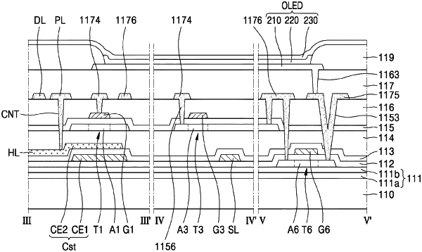
a first auxiliary thin film transistor that includes a first semiconductor layer that includes an oxide semiconductor material and a first gate electrode that overlaps the first semiconductor layer, and
a second auxiliary thin film transistor that includes a second semiconductor layer that includes Low Temperature Poly-Silicon (LTPS) and a second gate electrode that overlaps the second semiconductor layer.
|