| CPC H10K 50/858 (2023.02) [H10K 50/844 (2023.02); G09G 2300/0408 (2013.01); H10K 50/816 (2023.02); H10K 50/818 (2023.02); H10K 50/8445 (2023.02); H10K 59/12 (2023.02); H10K 59/1216 (2023.02); H10K 59/122 (2023.02); H10K 59/131 (2023.02); H10K 59/80516 (2023.02); H10K 59/80517 (2023.02); H10K 77/111 (2023.02); H10K 2102/311 (2023.02); H10K 2102/351 (2023.02)] | 26 Claims |

|
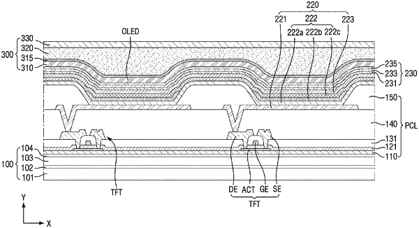
1. A display device comprising:
a substrate;
a display element on the substrate;
a capping layer on the display element; and
a thin film encapsulation layer on the capping layer,
wherein the capping layer includes:
a first capping layer on the display element;
a second capping layer on the first capping layer, the second capping layer having a refractive index greater than that of the first capping layer; and
a third capping layer on the second capping layer, such that the second capping layer is between the first capping layer and the third capping layer, the third capping layer having a refractive index smaller than that of the second capping layer,
wherein the second capping layer has a thickness of 30 nanometers (nm) to 60 nm, and
wherein the thin film encapsulation layer includes a first inorganic encapsulation layer, an auxiliary layer on the first inorganic encapsulation layer, and an organic encapsulation layer on the auxiliary layer.
|