| CPC H10K 50/844 (2023.02) [H10K 50/865 (2023.02); H10K 59/38 (2023.02); H10K 71/00 (2023.02)] | 4 Claims |
|
1. A preparation method for a display panel, comprising:
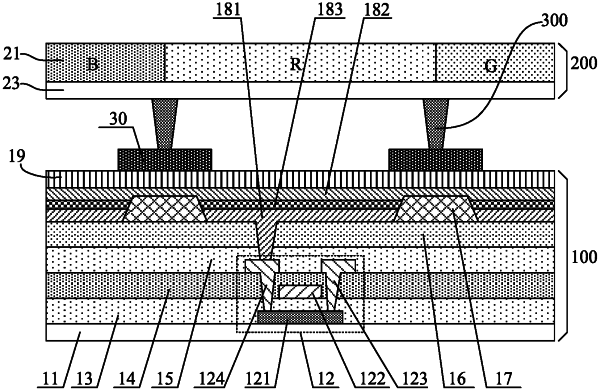
forming a display substrate panel and a cover panel which is aligned and combined into a cell with the display substrate panel; and
forming an isolation column disposed between the display substrate panel and the cover panel;
wherein forming the display substrate panel comprises:
forming multiple organic light-emitting diode (OLED) elements on a base substrate;
forming a thin film encapsulation layer on the OLED elements; and
forming a light blocking layer on the thin film encapsulation layer, wherein
the light blocking layer is located between two adjacent OLED elements, and thickness of the light blocking layer is less than or equal to 1.5 um;
the light blocking layer is formed at a process temperature less than or equal to 100° C.;
forming the light blocking layer on the thin film encapsulation layer comprises: forming a light blocking thin film on the thin film encapsulation layer; and performing exposure and development of the light blocking thin film by using a single-tone mask, to form a pattern of the light blocking layer;
metal traces are located between two adjacent OLED elements and disposed between the OLED elements and the base substrate, and an orthographic projection of the light blocking layer on the base substrate includes an orthographic projection of the metal traces on the base substrate;
forming the cover panel which is aligned and combined into the cell with the display substrate panel comprises: forming a color film layer disposed on a side of a second substrate of the cover panel facing the display substrate panel; and
forming the isolation column disposed between the display substrate panel and the cover panel comprises: forming the isolation column disposed between the light blocking layer of the display substrate panel and a protection layer of the cover panel, wherein the isolation column is in contact with the light blocking layer of the display substrate panel, and an orthographic projection of the isolation column on the base substrate is within a range of an orthographic projection of the light blocking layer on the base substrate.
|