| CPC H10K 50/828 (2023.02) [H10K 59/65 (2023.02); H10K 71/00 (2023.02)] | 17 Claims |

|
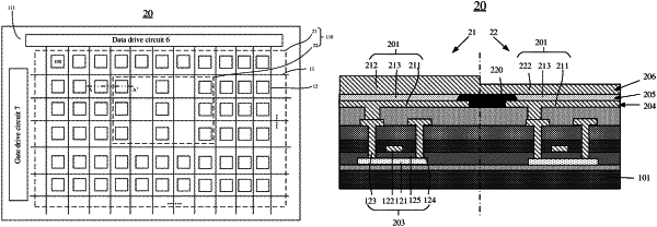
1. A display substrate, comprising a display area, the display area comprising a first display region and a second display region, the first display region having a pixel density higher than that of the second display region,
the display area comprising a base substrate, and a first electrode layer, a light-emitting functional layer, and a second electrode layer sequentially provided on the base substrate, the second electrode layer being provided on a side of the light-emitting functional layer away from the base substrate, and the first electrode layer and the second electrode layer being configured to apply a voltage to the light-emitting functional layer to enable the light-emitting functional layer to emit light,
wherein the second electrode layer comprises a first electrode portion provided in the first display region and a second electrode portion provided in the second display region, the first electrode portion and the second electrode portion are electrically connected with each other, and the second electrode portion has a light transmittance higher than that of the first electrode portion; and
the second electrode layer further comprises a third electrode portion between the first electrode portion and the second electrode portion, the third electrode portion is electrically connected with the first electrode portion and the second electrode portion, respectively, and a thickness of the third electrode portion decreases at first and then increases along a direction from the first display region to the second display region.
|