| CPC H10K 39/32 (2023.02) [H10K 19/20 (2023.02); H10K 30/30 (2023.02); H10K 30/82 (2023.02); H01L 27/14647 (2013.01)] | 20 Claims |

|
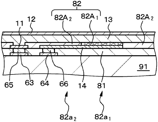
1. An imaging device, comprising:
a first electrode;
a charge storage electrode disposed at a distance from the first electrode;
a photoelectric conversion layer that is formed in contact with the first electrode and is located above the charge storage electrode, with an insulating layer being interposed between the charge storage electrode and the photoelectric conversion layer; and
a second electrode formed on the photoelectric conversion layer, wherein
a portion of the insulating layer located between the charge storage electrode and the photoelectric conversion layer includes a first region and a second region,
a portion of the insulating layer that occupies the first region is formed with a first insulating layer,
a portion of the insulating layer that occupies the second region is formed with a second insulating layer, and
an absolute value of fixed charge of a material forming the second insulating layer is smaller than an absolute value of fixed charge of a material forming the first insulating layer.
|
|
15. An imaging device, comprising:
a first electrode;
a charge storage electrode disposed at a distance from the first electrode;
a photoelectric conversion layer that is formed in contact with the first electrode and is located above the charge storage electrode, with an insulating layer being interposed between the charge storage electrode and the photoelectric conversion layer; and
a second electrode formed on the photoelectric conversion layer,
wherein an insulating material layer is provided between the first electrode and the charge storage electrode,
wherein a material forming the insulating material layer includes at least one of silicon oxynitride, silicon nitride, aluminum oxide, hafnium oxide, zirconium oxide, tantalum oxide, or titanium oxide,
wherein the material forming the insulating material layer has a different polarity from a polarity of carriers to be generated in the photoelectric conversion layer and to be sent to the first electrode,
wherein a second insulating material layer is provided in contact with at least part of a portion of the charge storage electrode not facing the first electrode, and
wherein a material forming the second insulating material layer includes at least one of aluminum oxide, hafnium oxide, zirconium oxide, tantalum oxide or titanium oxide.
|
|
19. An imaging device, comprising:
a first electrode;
a charge storage electrode disposed at a distance from the first electrode;
a photoelectric conversion layer that is formed in contact with the first electrode and is located above the charge storage electrode, with an insulating layer being interposed between the charge storage electrode and the photoelectric conversion layer; and
a second electrode formed on the photoelectric conversion layer,
wherein an insulating material layer is formed in contact with at least part of a portion of the charge storage electrode not facing the first electrode,
wherein a material forming the insulating material layer includes at least one of silicon oxynitride, silicon nitride, aluminum oxide, hafnium oxide, zirconium oxide, tantalum oxide, or titanium oxide,
wherein the material forming the insulating material layer has a same polarity as a polarity of carriers to be generated in the photoelectric conversion layer and to be sent to the first electrode,
wherein a second insulating material layer is provided between the first electrode and the charge storage electrode, and
wherein a material forming the second insulating material layer includes at least one of aluminum oxide, hafnium oxide, zirconium oxide, tantalum oxide or titanium oxide.
|