US 11,985,837 B2
Photoelectric conversion element
Shinnosuke Hattori, Tokyo (JP); Hajime Kobayashi, Tokyo (JP); Sae Miyaji, Tokyo (JP); Masato Kanno, Tokyo (JP); Miki Kimijima, Tokyo (JP); Yuta Hasegawa, Kanagawa (JP); Toshio Nishi, Tokyo (JP); Takashi Kawashima, Tokyo (JP); Yosuke Saito, Tokyo (JP); and Yuta Inaba, Tokyo (JP)
Assigned to Sony Corporation, Tokyo (JP); and Sony Semiconductor Solutions Corporation, Kanagawa (JP)
Appl. No. 17/261,215
Filed by SONY CORPORATION, Tokyo (JP); and SONY SEMICONDUCTOR SOLUTIONS CORPORATION, Kanagawa (JP)
PCT Filed Jul. 25, 2019, PCT No. PCT/JP2019/029184
§ 371(c)(1), (2) Date Jan. 19, 2021,
PCT Pub. No. WO2020/022421, PCT Pub. Date Jan. 30, 2020.
Claims priority of application No. 2018-140401 (JP), filed on Jul. 26, 2018; and application No. 2019-133395 (JP), filed on Jul. 19, 2019.
Prior Publication US 2021/0280639 A1, Sep. 9, 2021
Int. Cl. H01L 27/146 (2006.01); H10K 30/81 (2023.01); H10K 39/32 (2023.01)
CPC H10K 39/32 (2023.02) [H01L 27/14621 (2013.01); H01L 27/14625 (2013.01); H10K 30/81 (2023.02)] 24 Claims
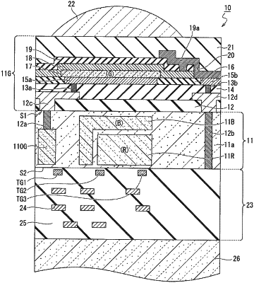
OG exemplary drawing
 
1. A photoelectric conversion element, comprising:
a first electrode and a second electrode arranged to face each other; and
a photoelectric conversion layer provided between the first electrode and the second electrode, wherein
the photoelectric conversion layer includes a first organic semiconductor material and a second organic semiconductor material, and
at least one of the first organic semiconductor material or the second organic semiconductor material is an organic molecule having a highest occupied molecular orbital (HOMO) volume fraction of 0.15 or less or a lowest unoccupied molecular orbital (LUMO) volume fraction of 0.15 or less.