| CPC H10B 43/35 (2023.02) [H01L 29/6684 (2013.01); H01L 29/78391 (2014.09); H10B 51/20 (2023.02)] | 19 Claims |
|
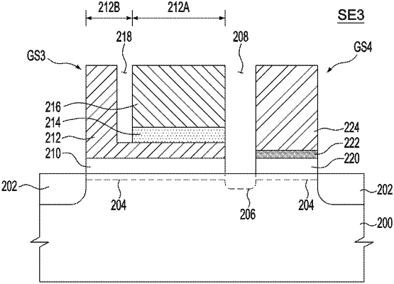
1. A switching element comprising:
a first gate dielectric layer formed over a substrate;
a second gate dielectric layer formed over the first gate dielectric layer to overlap a part of the first gate dielectric layer, and including a ferroelectric material;
a second gate electrode formed over the second gate dielectric layer; and
a first gate electrode located between the first and second gate dielectric layers, and configured to control the second gate dielectric layer to selectively have negative capacitance,
wherein the first gate electrode comprises a first region located between the first and second gate dielectric layers and a second region extended from the first region and neighboring a sidewall of the second gate electrode with a gap provided therebetween.
|