| CPC H10B 43/27 (2023.02) [H01L 29/24 (2013.01); H01L 29/40117 (2019.08); H01L 29/66969 (2013.01); H01L 29/7831 (2013.01); H01L 29/7889 (2013.01); H10B 41/27 (2023.02); H10B 41/35 (2023.02); H10B 41/41 (2023.02); H10B 43/20 (2023.02); H10B 43/35 (2023.02); H01L 21/02565 (2013.01); H01L 21/0262 (2013.01); H10B 43/40 (2023.02)] | 6 Claims |
|
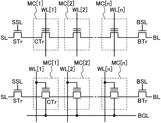
1. A semiconductor device comprising:
a first insulator;
a first conductor over the first insulator;
a second insulator over the first conductor;
a second conductor over the second insulator;
a third insulator enclosed by the first conductor;
a first semiconductor enclosed by the third insulator;
a fourth insulator enclosed by the first semiconductor;
a fifth insulator enclosed by the first semiconductor in a region enclosed by the first conductor;
a second semiconductor enclosed by the fifth insulator; and
a sixth insulator enclosed by the second semiconductor;
wherein the third insulator, the first semiconductor, the fifth insulator, the second semiconductor and the sixth insulator penetrate a stack comprising the first insulator, the first conductor, the second insulator and the second conductor in a first portion,
wherein a side of the second conductor protrudes inward of the first portion compared to a side of the first conductor,
wherein the first semiconductor comprises:
a first region enclosed by the first insulator;
a second region enclosed by the first conductor;
a third region enclosed by the second insulator; and
a fourth region enclosed by the second conductor; and
wherein each of the first region, the third region and the fourth region comprises a region with a higher conductivity than the second region.
|