| CPC H10B 43/27 (2023.02) [H10B 43/10 (2023.02); H10B 43/35 (2023.02)] | 20 Claims |

|
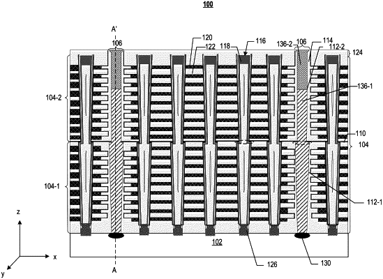
1. A method for forming a memory device, comprising:
forming holes extending vertically in a first dielectric deck comprising interleaved first sacrificial layers and first dielectric layers over a substrate;
forming sacrificial source contact structures in the holes;
forming a second dielectric deck comprising interleaved second sacrificial layers and second dielectric layers over the first dielectric deck;
forming a slit opening extending vertically and laterally in the second dielectric deck, the slit opening being aligned with and exposing the sacrificial source contact structures;
removing the sacrificial source contact structures through the slit opening such that the slit opening is interconnected with the holes; and
forming a source contact structure in the slit opening and the holes.
|