| CPC H10B 43/27 (2023.02) [H10B 41/10 (2023.02); H10B 41/20 (2023.02); H10B 43/10 (2023.02); H10B 43/20 (2023.02); H10B 41/27 (2023.02)] | 8 Claims |
|
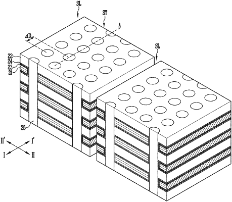
1. A semiconductor device comprising:
a first slit insulating layer and a second slit insulating layer spaced apart from each other;
insulating layers stacked on top of each other and disposed between the first and second slit insulating layers;
conductive layers stacked on top of each other and interposed between the insulating layers, each of the conductive layers including a first portion adjacent to the first slit insulating layer, a second portion adjacent to the second slit insulating layer and a third portion between the first portion and the second portion;
pillars passing through the insulating layers and the conductive layers;
a barrier pattern interposed between each of the conductive layers and each of the insulating layers and extending between each of the conductive layers and each of the pillars;
a first deposition inhibiting pattern contacting the first slit insulating layer and interposed between the barrier pattern and the first portion in each of the conductive layers; and
a second deposition inhibiting pattern contacting the second slit insulating layer and interposed between the barrier pattern and the second portion in each of the conductive layers,
wherein the first deposition inhibiting pattern and the second deposition inhibiting pattern are spaced apart from each other by the third portion in each of the conductive layers, and
wherein the first portion, the second portion and the third portion in each of the conductive layers are connected to each other without interposing the first and second deposition inhibiting patterns.
|