| CPC H10B 41/40 (2023.02) [H10B 41/10 (2023.02); H10B 41/27 (2023.02); H10B 41/35 (2023.02); H10B 43/10 (2023.02); H10B 43/27 (2023.02); H10B 43/35 (2023.02); H10B 43/40 (2023.02)] | 20 Claims |
|
1. A semiconductor device, comprising:
a peripheral circuit structure including a first substrate and at least one of active devices or passive devices on the first substrate;
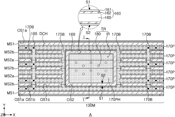
a memory cell structure including a second substrate on the peripheral circuit structure and having a first region and a second region, the memory cell structure including gate electrodes stacked on the first region spaced apart from each other in a first direction, and extending in a second direction and arranged in a staircase shape on the second region, the memory cell structure including interlayer insulating layers alternately stacked with the gate electrodes, the memory cell structure including channel structures penetrating the gate electrodes that extend in the first direction, each of the channel structures including a channel layer, and the memory cell structure including isolation regions penetrating the gate electrodes, extending in the second direction, and spaced apart from each other in a third direction;
a through wiring region including sacrificial insulating layers on the second region, spaced apart from the gate electrodes, and alternately stacked with the interlayer insulating layers, the through wiring region including a through contact plug penetrating the sacrificial insulating layers and electrically connecting the gate electrodes to the active or passive devices; and
a barrier structure surrounding the through wiring region and including a core insulating layer, a first barrier layer, and a second barrier layer,
wherein the core insulating layer is in a central region of the barrier structure and includes silicon oxide,
the second barrier layer covers side surfaces of the core insulating layer and a bottom surface of the core insulating layer, and
the first barrier layer covers external side surfaces of the second barrier layer and a bottom surface of the second barrier layer.
|