| CPC H10B 20/20 (2023.02) [G11C 17/165 (2013.01); H01L 23/5252 (2013.01); G11C 2213/79 (2013.01)] | 20 Claims |

|
1. A memory device comprising:
an anti-fuse cell array having a plurality of anti-fuse cells, each of the plurality of anti-fuse cells comprising:
a first transistor; and
a second transistor connected to the first transistor,
wherein a first terminal of the first transistor is connected to a bit line;
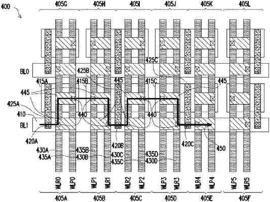
wherein the bit line is a buried rail formed in a substrate of the first transistor and the second transistor;
wherein the bit line is connected to a first active region of the first terminal;
wherein the bit line is connected to the first active region through a first metal over oxide layer;
wherein the bit line is further connected to a first edge metal over oxide layer at a first end of the bit line and a second edge metal over oxide layer at a second end of the bit line;
wherein the first edge metal over oxide layer is connected to the second metal over oxide layer through an interconnect layer; and
wherein the anti-fuse cell array is protected by a first protection block comprising at least one first dummy polysilicon region that is either floating or connected to ground.
|