| CPC H10B 12/30 (2023.02) [H10B 12/01 (2023.02)] | 16 Claims |
|
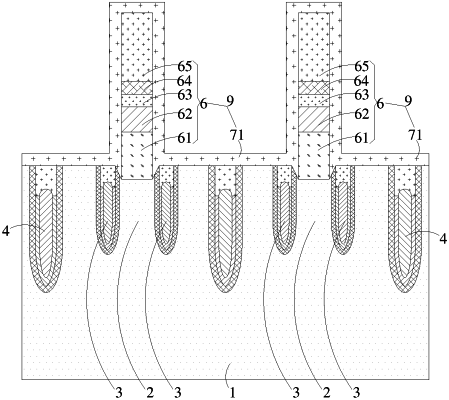
1. A semiconductor device, comprising:
a semiconductor substrate, wherein a plurality of strip-shaped stacked structures and a sidewall structure covering a periphery of each of the plurality of strip-shaped stacked structures are disposed on the semiconductor substrate, and a conductive structure is disposed on a side of each of the plurality of strip-shaped stacked structures far away from the semiconductor substrate; and
wherein each of the plurality of strip-shaped stacked structures comprises:
a conductor layer, disposed on the semiconductor substrate and configured to transmit a data signal;
an isolation layer, disposed on a side of the conductor layer away from the semiconductor substrate;
a separation layer, disposed on a side of the isolation layer away from the semiconductor substrate and being made of a low dielectric constant material; and
a dielectric layer, disposed on a side of the separation layer away from the semiconductor substrate and configured to isolate the separation layer from the conductive structure.
|