US 11,985,809 B2
Memory device having electrically floating body transistor
Yuniarto Widjaja, San Jose, CA (US); Jin-Woo Han, San Jose, CA (US); and Benjamin S. Louie, Fremont, CA (US)
Assigned to Zeno Semiconductor, Inc., Sunnyvale, CA (US)
Filed by Zeno Semiconductor, Inc., Sunnyvale, CA (US)
Filed on Jul. 18, 2022, as Appl. No. 17/867,593.
Application 14/955,339 is a division of application No. 13/746,523, filed on Jan. 22, 2013, granted, now 9,230,651, issued on Jan. 5, 2016.
Application 17/867,593 is a continuation of application No. 17/207,687, filed on Mar. 21, 2021, granted, now 11,417,657.
Application 17/207,687 is a continuation of application No. 16/827,373, filed on Mar. 23, 2020, granted, now 10,978,455, issued on Apr. 13, 2021.
Application 16/827,373 is a continuation of application No. 16/224,534, filed on Dec. 18, 2018, granted, now 10,629,599, issued on Apr. 21, 2020.
Application 16/224,534 is a continuation of application No. 15/867,877, filed on Jan. 11, 2018, granted, now 10,192,872, issued on Jan. 29, 2019.
Application 15/867,877 is a continuation of application No. 15/403,757, filed on Jan. 11, 2017, granted, now 9,893,067, issued on Feb. 13, 2018.
Application 15/403,757 is a continuation of application No. 14/955,339, filed on Dec. 1, 2015, granted, now 9,576,962, issued on Feb. 21, 2017.
Claims priority of provisional application 61/621,546, filed on Apr. 8, 2012.
Prior Publication US 2022/0359522 A1, Nov. 10, 2022
Int. Cl. H10B 12/00 (2023.01); G11C 11/404 (2006.01); G11C 16/04 (2006.01); G11C 16/10 (2006.01); G11C 16/26 (2006.01); G11C 16/34 (2006.01); H01L 29/08 (2006.01); H01L 29/10 (2006.01); H01L 29/36 (2006.01); H01L 29/70 (2006.01); H01L 29/73 (2006.01); H01L 29/732 (2006.01); H01L 29/78 (2006.01); H10B 12/10 (2023.01); H10B 41/35 (2023.01)
CPC H10B 12/20 (2023.02) [G11C 11/404 (2013.01); G11C 16/0433 (2013.01); G11C 16/10 (2013.01); G11C 16/26 (2013.01); G11C 16/3427 (2013.01); H01L 29/0804 (2013.01); H01L 29/0821 (2013.01); H01L 29/1095 (2013.01); H01L 29/36 (2013.01); H01L 29/70 (2013.01); H01L 29/73 (2013.01); H01L 29/7302 (2013.01); H01L 29/7841 (2013.01); H10B 12/10 (2023.02); H10B 41/35 (2023.02); H01L 29/1004 (2013.01); H01L 29/732 (2013.01)] 20 Claims
OG exemplary drawing
 
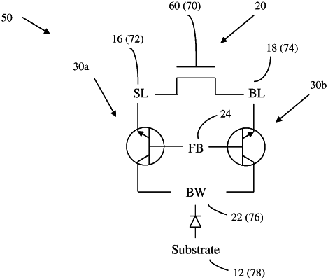
1. A semiconductor memory cell comprising:
a first bipolar device having a first floating base region, a first collector region, and a first emitter, and
a second bipolar device having a second floating base region, a second collector region, and a second emitter,
wherein said first floating base region is common to said second floating base region,
wherein said first collector region is common to said second collector region, and
a transistor comprising said first emitter, said first floating body region, and said second emitter,
wherein a state of said semiconductor memory cell is maintained through a back bias applied to said first and second collector regions;
wherein current flow through said transistor during a read operation is determined by said state of said semiconductor memory cell;
wherein said first and second collector regions are commonly connected to at least two of said memory cells; and
wherein said first and second collector regions have a band gap that is lower than a band gap of said first and second floating base regions.