US 11,985,806 B2
Vertical 2-transistor memory cell
Kamal M. Karda, Boise, ID (US); Srinivas Pulugurtha, Boise, ID (US); Haitao Liu, Boise, ID (US); Karthik Sarpatwari, Boise, ID (US); and Durai Vishak Nirmal Ramaswamy, Boise, ID (US)
Assigned to Micron Technology, Inc., Boise, ID (US)
Filed by Micron Technology, Inc., Boise, ID (US)
Filed on Dec. 19, 2019, as Appl. No. 16/721,380.
Claims priority of provisional application 62/785,119, filed on Dec. 26, 2018.
Prior Publication US 2020/0212045 A1, Jul. 2, 2020
This patent is subject to a terminal disclaimer.
Int. Cl. H01L 27/108 (2006.01); H10B 12/00 (2023.01); G11C 11/402 (2006.01)
CPC H10B 12/01 (2023.02) [G11C 11/4023 (2013.01)] 35 Claims
OG exemplary drawing
 
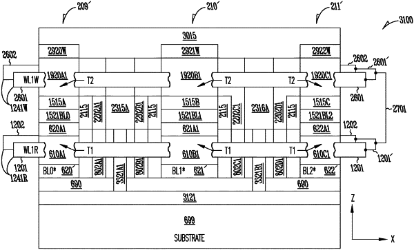
1. A method comprising:
forming a first transistor of a memory cell over a substrate, including forming a channel region of the first transistor;
forming a memory element of the memory cell on at least one side of the channel region of the first transistor, such that the memory element is separated from the channel region of the first transistor by a dielectric material; and
forming a second transistor of the memory cell, including forming a channel region of the second transistor, such that the channel region of the second transistor is coupled to the memory element.