| CPC H05K 9/0032 (2013.01) [H05K 1/023 (2013.01); H05K 1/188 (2013.01); H05K 3/284 (2013.01); H05K 2201/0715 (2013.01); H05K 2203/1377 (2013.01)] | 27 Claims |
|
1. A package comprising:
a substrate;
a first integrated device coupled to the substrate;
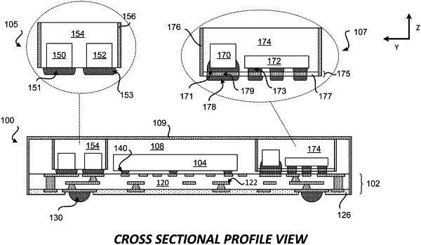
a first block device coupled to the substrate through a first plurality of solder interconnects, the first block device comprising:
a first electrical component;
a second electrical component;
a first encapsulation layer encapsulating the first electrical component and the second electrical component, wherein the first encapsulation layer comprises a first surface; and
a first metal layer coupled to and touching a lateral surface of the first encapsulation layer, wherein an entire portion of the first metal layer of the first block device, between a second metal layer and a bottom portion of the first block device, extends along a vertical plane;
a second encapsulation layer at least partially encapsulating the first integrated device and the first block device, wherein the second encapsulation layer comprises a second surface that shares a same horizontal plane as the first surface of the first encapsulation layer;
the second metal layer located at least over the first block device, directly coupled to and touching (i) the first surface of the first encapsulation layer of the first block device, (ii) the second surface of the second encapsulation layer, and (iii) the first metal layer; and
a second block device coupled to the substrate, wherein the second block device comprises:
a third electrical component;
a third encapsulation layer encapsulating the third electrical component, wherein the third encapsulation layer comprises a third surface that shares the same horizontal plane as (i) the first surface of the first encapsulation layer and (ii) the second surface of the second encapsulation layer; and
a third metal layer coupled to and touching (i) a lateral surface of the third encapsulation layer and (ii) the second metal layer, wherein the third metal layer is configured as a shield for the second block device.
|