| CPC H05K 1/0203 (2013.01) [H01L 23/3128 (2013.01); H01L 23/5383 (2013.01); H01L 23/5386 (2013.01); H01L 23/5389 (2013.01); H01L 23/552 (2013.01); H01L 23/66 (2013.01); H01L 24/20 (2013.01); H01Q 1/38 (2013.01); H05K 1/0216 (2013.01); H05K 1/0277 (2013.01); H05K 1/144 (2013.01); H05K 1/181 (2013.01); H01L 2223/6677 (2013.01); H01L 2224/214 (2013.01); H05K 2201/10356 (2013.01); H05K 2201/10378 (2013.01)] | 10 Claims |

|
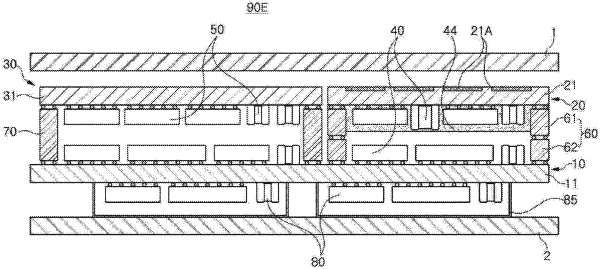
1. A printed circuit board assembly, comprising:
a first printed circuit board having a first surface and a second surface opposing the first surface;
a second printed circuit board disposed on the first surface of the first printed circuit board and including an antenna pattern disposed on a first surface of the second printed circuit board;
a first electronic component disposed on a second surface of the second printed circuit board opposing the first surface of the second printed circuit board;
a second electronic component disposed on the first surface of the first printed circuit board;
a first interposer substrate disposed around the first and second electronic components and electrically connecting the first printed circuit board and the second printed circuit board to each other;
a third printed circuit board disposed on the first surface of the first printed circuit board and spaced apart from the second printer circuit board;
a third electronic component disposed on a surface of the third printed circuit board;
a fourth electronic component disposed on the first surface of the first printed circuit board; and
a second interposer substrate disposed around the third and fourth electronic components and electrically connecting the first printed circuit board and the third printed circuit board to each other,
wherein the first printed circuit board, the second electronic component, the first electronic component, and the second printed circuit board are sequentially disposed, and
wherein the first printed circuit board, the fourth electronic component, the third electronic component and the third printed circuit board are sequentially disposed.
|