| CPC H04N 25/77 (2023.01) [H01L 27/14614 (2013.01); H01L 27/14643 (2013.01); A61B 1/05 (2013.01); G02B 23/2407 (2013.01); H01L 27/14625 (2013.01); H01L 27/1463 (2013.01); H01L 27/14683 (2013.01)] | 19 Claims |
|
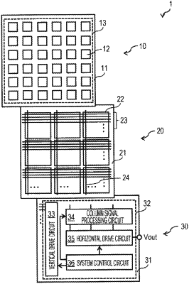
1. A solid-state image sensor comprising:
a first semiconductor substrate having a photoelectric conversion element; and
a second semiconductor substrate facing the first semiconductor substrate with an insulating film interposed therebetween,
wherein the second semiconductor substrate has an amplification transistor that amplifies an electrical signal output from the photoelectric conversion element on a first main surface, has a region having a resistance lower than a resistance of the second semiconductor substrate on a second main surface opposite to the first main surface, and is grounded via the region,
wherein the second semiconductor substrate has a certain conductive type, and
wherein the region with a lower resistance includes a higher concentration of impurities than other regions of the second semiconductor substrate.
|