| CPC H04N 25/745 (2023.01) [H04N 25/779 (2023.01); H04N 25/7795 (2023.01); H04N 25/79 (2023.01)] | 20 Claims |
|
1. An image sensor, comprising:
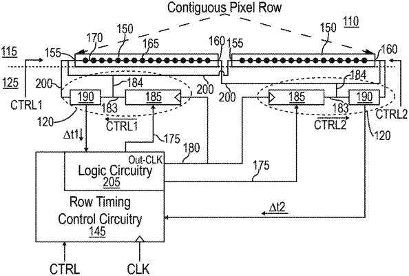
a pixel array comprising a plurality of rows, wherein a first row comprises a first pixel group and a second pixel group, wherein the first pixel group has first and second opposing ends, and wherein the second pixel group has first and second opposing ends;
a first row driver circuit connected to the first end of the first pixel group;
a second row driver circuit connected to the second end of the second pixel group;
a first delay measurement circuit that has a first input connected directly to the first row driver circuit and a second input connected directly to a first node that is interposed between the first end of the first pixel group and the first row driver circuit; and
a second delay measurement circuit that has a first input connected directly to the second row driver circuit and a second input connected directly to a second node that is interposed between the second end of the second pixel group and the second row driver circuit.
|