| CPC H04N 25/46 (2023.01) [G01S 7/4816 (2013.01); G01S 17/894 (2020.01); H04N 25/44 (2023.01); H04N 25/441 (2023.01); H04N 25/705 (2023.01); H04N 25/75 (2023.01)] | 42 Claims |
|
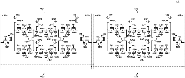
1. A time-of-flight pixel array, comprising:
a plurality of photodiodes configured to generate charge in response to reflected modulated light incident upon the plurality of photodiodes;
a plurality of transfer transistors coupled to the plurality of photodiodes, wherein the plurality of transfer transistors includes a plurality of first transfer transistors and a plurality of second transfer transistors, wherein the plurality of first transfer transistors is configured to transfer a first portion of the charge from the plurality of photodiodes in response to a first modulation signal, wherein the plurality of second transfer transistors is configured to transfer a second portion of the charge from the plurality of photodiodes in response to a second modulation signal, wherein the second modulation signal is an inverted first modulation signal;
a plurality of floating diffusions, wherein the plurality of floating diffusions includes a plurality of first floating diffusions coupled to the plurality of first transfer transistors;
a plurality of binning transistors, wherein the plurality of binning transistors includes a plurality of first binning transistors, wherein a first one of the plurality of first binning transistors is coupled between a first one of the plurality of first floating diffusions and a second one of the plurality of first floating diffusions;
a plurality of sample and hold transistors, wherein the plurality of sample and hold transistors includes a plurality of first sample and hold transistors coupled to the plurality of first floating diffusions; and
a plurality of memory nodes, wherein the plurality of memory nodes includes a plurality of first memory nodes, wherein a first one of the plurality of first memory nodes is coupled to the first one of the plurality of first floating diffusions through a first one of the plurality of first sample and hold transistors, wherein a second one of the plurality of first memory nodes is coupled to the second one of the plurality of first floating diffusions through a second one of the plurality of first sample and hold transistors.
|