| CPC H03H 7/0115 (2013.01) [H03H 7/0153 (2013.01); H04B 1/0458 (2013.01); H04B 1/18 (2013.01); H04B 1/40 (2013.01); H03H 2007/013 (2013.01)] | 19 Claims |
|
1. A wireless transceiver, comprising:
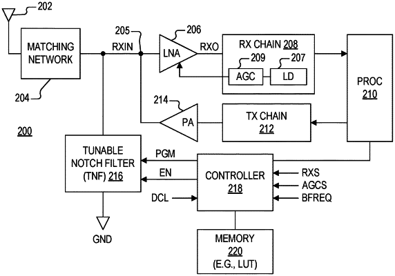
a receiver circuit coupled to a radio frequency transceiver node;
a tunable notch filter coupled between the radio frequency transceiver node and a reference node, wherein the tunable notch filter comprises a digitally programmable capacitor;
a memory programmed with a plurality of digital values, wherein the plurality of digital values are predetermined during a procedure performed by the wireless transceiver based on at least one blocker signal; and
a controller that programs the digitally programmable capacitor of the tunable notch filter with a digital value selected from the memory based on a blocker frequency signal and that selectively enables the tunable notch filter based on a receive state of the wireless transceiver and a gain control state of the receiver circuit to attenuate the at least one blocker signal.
|