| CPC H03F 3/70 (2013.01) [G01R 27/2605 (2013.01); H03F 3/45968 (2013.01); H03F 2200/375 (2013.01)] | 20 Claims |
|
1. A circuit, comprising:
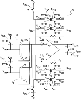
an amplifier having a first input node and a second input node configured to be coupled to opposite ends of at least one capacitance to detect a capacitive variation signal indicative of variations in a capacitance value of the at least one capacitance, the amplifier having a first output node and a second output node,
a bias voltage node configured to provide a bias voltage level,
a first set of switches configured, based on a first reset signal having a first value, to couple the first and second input nodes of the amplifier to the bias voltage node and to couple therebetween the first and second output nodes of the amplifier,
a first feedback branch coupled between the first output node and the first input node of the amplifier, the first feedback branch including a first RC network including a first and a second capacitance,
a second feedback branch coupled between the second output node and the second input node of the amplifier, the second feedback branch including a second RC network including a third and a fourth capacitance,
the first and second feedback branches further including:
a second set of switches intermediate to the first and second input nodes of the amplifier and the first, second, third and fourth capacitances, and
a third set of switches intermediate to the first and second output nodes of the amplifier and the first, second, third and fourth capacitances,
wherein
the switches in the second set of switches are configured to selectively couple one of the first and second capacitances in the first feedback branch and one of the third and fourth capacitances in the second feedback branch to the first and second input nodes of the amplifier based on a second reset signal having a first value, and
the switches in the third set of switches are configured to selectively couple said one of the first and second capacitances in the first feedback branch and said one of the third and fourth capacitances in the second feedback branch to the first and second output nodes of the amplifier based on a second reset signal having a first value,
wherein the first reset signal is configured to have a first value for a first time interval and to switch from the first value to a second value after the first time interval, and wherein, in response to the first reset signal switching from the first value to the second value, the second reset signal maintains said first value for a further time interval exceeding the first time interval during which the first reset signal has the first value.
|