| CPC H03F 1/0277 (2013.01) [H03F 1/086 (2013.01); H03F 1/565 (2013.01); H03F 3/193 (2013.01); H03F 3/195 (2013.01); H03F 3/72 (2013.01); H03F 2200/111 (2013.01); H03F 2200/18 (2013.01); H03F 2200/213 (2013.01); H03F 2200/222 (2013.01); H03F 2200/225 (2013.01); H03F 2200/243 (2013.01); H03F 2200/252 (2013.01); H03F 2200/294 (2013.01); H03F 2200/297 (2013.01); H03F 2200/301 (2013.01); H03F 2200/306 (2013.01); H03F 2200/321 (2013.01); H03F 2200/387 (2013.01); H03F 2200/391 (2013.01); H03F 2200/399 (2013.01); H03F 2200/411 (2013.01); H03F 2200/42 (2013.01); H03F 2200/429 (2013.01); H03F 2200/451 (2013.01); H03F 2200/48 (2013.01); H03F 2200/489 (2013.01); H03F 2200/492 (2013.01); H03F 2200/525 (2013.01); H03F 2200/61 (2013.01); H03F 2200/75 (2013.01); H03F 2203/7206 (2013.01); H03F 2203/7209 (2013.01); H03F 2203/7233 (2013.01)] | 22 Claims |
|
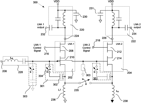
1. An amplifier including:
(a) a plurality of independently-controlled low noise amplifiers (LNA), each including at least an input transistor having a gate and a source terminal;
(b) at least one gate capacitance module, each having a first terminal coupled to the gate of an associated input transistor of one of the independently-controlled LNAs, and a second terminal coupled to the source terminal of the associated input transistor; and
(c) a source switch coupled between the source terminal of the input transistor of a first of the independently-controlled LNAs and the source terminal of the input transistor of a second of the independently-controlled LNAs, the source switch configured to connect the source terminals while only one of the first and second independently-controlled LNAs is enabled, and disconnect the source terminals while both of the first and second independently-controlled LNAs are enabled;
wherein each gate capacitance module is configured to connect a capacitance between the gate and source terminal of the associated input transistor in a first mode of operation, and disconnect the capacitance in a second mode of operation.
|